Frequency synthesizer for transceiver. SDR and Retro by RA3PKJ
25.10.2015
The assembly of a completely new design - an SDR transceiver from UT3MK, started with a frequency synthesizer. Next, the assembly of the transceiver board itself, DFT filters and, possibly, an amplifier will follow ... There is an idea to make a full-fledged device using the achievements of a talented radio amateur - UT3MK.
The variant of the circuit solution was discussed in this thread. I decided to build the 13th version of the synthesizer. The synthesizer and transceiver board was kindly made by Victor RA3AIW, for which many thanks to him. Also, he will help launch the device, like a radio amateur who has successfully repeated, including this design ...
All components were purchased from the chipdip store, except for the Si570, which was left over from a Peaberry RX-TX Sound SDR transceiver. By the way, you can buy it on sdr-kits without any problems.
Photos of the assembly process will be posted.
Today the board was drilled.


Before sealing the main chips, the operating voltage is checked, the synthesizer supply voltage is adjusted (3.3V in my case). Then all the cases are soldered, except for the Si570, the board is passed through with a hairdryer, washed, and visually controlled. Further, test firmware is uploaded and, in case of successful operation of all functions, the synthesizer is soldered. To upload firmware - you will need to make a programmer for ATmega32. I want to try to make the simplest option for the LPT port.
27.10.2015
All parts except Si570 are soldered. The ATmega32 slightly turned counterclockwise, but I don't think it's a big deal... First, the contacts under the chips were tinned after applying the LTI solution. Then, they warmed up with a hairdryer to evenly distribute the tin. Further, again LTI and tacking the chips by the extreme legs with a soldering iron. Further, heating each side with a hairdryer, LTI, adding tin with a soldering iron tip, again LTI and final heating with a hairdryer. For myself, I chose this method of sealing cases ...

After the board is fully operational (and I really hope that this will happen), the rest of the assembly will be warmed up with preliminary application of LTI and the final washing of the board.

The voltage is set to 3.3V on the 7th leg of the Si570. When connecting the board to the computer via USB, a new device was found, which under WinXP asked for a driver. The drivers have been installed.

The next step is to make a programming cable for the LPT port and try to upload a test firmware ...
29.10.2015
A loop was made to the LPT port. Since, for good, they only need to be used a couple of times - I did not bother with the aesthetics of the design. The main thing is that the interface cable does its job.

At first, with the version posted on the ponyprog website, it was not possible to flash it. The interface of the program was different and the required version of ATmega32 was not in the menu. Then, I downloaded the version from Yuri's website using the link from the docks for atmega firmware and everything was successfully flashed in two seconds. Further, I set and recorded the fuses, read them and began to test the device through PowerSDR 2.5.3. All functions worked without problems. After that, I erased the memory, uploaded the working version of the firmware (Madeira-6) and soldered the Si570. By the way, she also turned and also counterclockwise. I didn't give a damn...

At first everything worked fine. CAT kept in touch, the encoder worked, etc. The only thing is that for a very long time I could not calibrate the frequency, which differed from the reference one by about 2 kHz. As it turned out later, the reason for this was a malfunction in one of the channels of the SDR receiver, which gave a 100% DSLR in the panorama.
To calibrate and suppress the DSLR, I use a 7.3728 MHz crystal oscillator. By the way, these generators have a fairly high output level (I set 1:100) and a very low level of phase noise - the signal peak is clearly visible on the screen and the frequency strictly corresponds to that indicated on the quartz case ...
Unfortunately, after further experiments, the CAT connection began to act up and then fell off altogether. Reinstalling the drivers, changing the COM port number, uninstalling PowerSDR with cleaning the registry and contents in hidden folders, did not give anything, which greatly upset and spoiled the mood ...
30.10.2015
Today it was noticed that the problem with the failure was due to a violation of the contact (s) in some place on the board (by bending it in different directions). I had to solder some parts and warm up the entire board with a hot air gun (which had not been done until that moment) and everything worked stably.
Also, a defect was fixed in one of the receiver channels (by the way, the one that is mainly used on Web-SDR). After that, the program was calibrated in terms of level and mirror suppression. To set hardware suppression in the receiver, version 1.18.6 of the program was used, when the mirror was not yet suppressed in the machine. The suppression was about 45dB.

After that, I returned to version 2.3.5.

We used an integrated sound card at 48kHz, which has all its inherent drawbacks... This is the reason for the sticks on the edges of the zero IF, which also makes a lot of noise.
Having played a little with the reception of the air, today, I decided to dwell on the results achieved ...

There was a large number of sticks on the panorama. According to previous experience, this misfortune, to a large extent, disappeared after the structure was placed in a metal screen ...
31.10.2015
Well, the synthesizer works stably, the board is washed from the flux. Tasa's receiver has returned to WebSDR again, with a shielded case, this time. There is an assembled main board of the transceiver version 3B, there is a signet and all components for version 2A. Apparently, I will continue to assemble the DFT board - the 3rd component of the future SDR transceiver, if the creative search does not lead in the other direction ...
01.11.2015
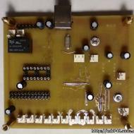
Today I put together a 3B version board and this synthesizer.
![]()
Some functions of the synthesizer are not used yet. Also, there are no filters and amplifier. At the output, with an acceptable quality of a two-tone signal, we have about 1V of the amplitude RF voltage. On the whole, I am satisfied with the formation of the SSB signal band, but it needs to be filtered ... There is an idea to try to assemble DFTs and a preamplifier in a similar package.
04.11.2015
Today I made a BPF filter for a range of 40m. The scheme is also taken from Yuri's website. Modeled this filter in RFSimm99. However, after making it and carefully measuring all the elements with an L / C meter, it turned out that the filter bandwidth was shifted higher by about 1 MHz. I had to select containers and, in the end, the following result was obtained:

As it turned out later, the calibration of the L / C-meter was knocked down and all measurements of inductances were incorrect ... I plan, later, to measure and redo the filter again.
I don't have an NWT-7 gauge yet, but my AA-330M will do just fine for this task. In principle, it shows the reverse picture, as I see it. And, using the SWR on the graph, you can determine the filter bandwidth ... The measurement technique is simple - a non-inductive load is connected to the filter input - a resistance of 50 Ohm (two MLT-2 100 Ohm in parallel), the filter output is connected to the analyzer and the entire range is scanned.
The scarf for BPF is designed for 3 filters. I plan to do more bands 80m and 20m. The scarf was placed inside the case.

I have an idea to place a small OPA2764 or AD8009 preamplifier in the remaining space to get 1W output from the device...
09.11.215
Modeled bandpass filters for 20m and 80m.

Here and in other filters, I selected the values of the elements by simple enumeration.

10.11.2015
For the 80m range, I made an LPF filter, in haste.

Since yesterday, the transceiver has been working as part of a WebSDR receiver, in test mode. The essence of the idea is to switch reception to different bands, depending on the time of day (taking into account the characteristics of the passage) and check the stability of the operation of the transceiver nodes. The process of managing all components of the system takes place remotely, through remote access to computers.
13.04.2017
From the experience of operating this synthesizer. The advantages include advanced switching and control capabilities, the presence of a rotary encoder and light indication. I see two obvious disadvantages. The most important is the busy com-port and the impossibility of docking the synthesizer program with log programs (I use UR5EQF). It seems that you can use software splitters to run various applications through one com port, but I have not tried this feature yet. The second, significant, minus is the inability to connect a telegraph key or a manipulator.
To be continued...
Simple, versatile synthesizer based on Si5351 up to 160 MHz.
The Si5351A is an oscillator with three independent outputs that can generate each individual signal from 8 kHz to 160 MHz. The SiLabs Si5351A chip is the cousin of the well-known and popular Si570 but much smaller and much cheaper. Unlike Si570, Si5351A does not have a quartz crystal inside. The reference frequency can be 25MHz or 27MHz. Can be used as a crystal oscillator or a crystal resonator. Si5351A which uses I2C interface is easy to use with Arduino microcontroller. All these features, together with the software library, make it easy and quick to set up the Si5351A for use on your next project to suit your needs. Three independent outputs are ideal for use as a VFO in a superheterodyne or transceiver. The small 1 Hz tuning step and wide frequency range make it an excellent choice for projects such as receivers, transceivers, direct conversion or SDR techniques, antenna analyzers, signal generators or clock generators. The optional TCXO makes the Si5351A especially useful in applications where high stability is required, such as in a WSPR or QRSS transmitter.

The proposed synthesizer is intended for use in simple home-made receivers, transceivers with a quartz filter, in the direct conversion technique, SDR - a technique where the condition for their operation is doubling or quadrupling (X2, X4) the frequency at the output of the synthesizer. Moreover, for premo - transmitting devices with one IF in the region of 9 MHz (it can be any), the necessary frequencies of the "support" are "removed" from the additional output of the Si5351. This makes it possible to abandon the classic quartz reference oscillators with frequency-tuning - shifting circuits, capacitors to select the desired sideband. And with minimal (no) knowledge, the user himself can change, adjust their values.

It will also not be difficult to choose the mode of operation of the synthesizer that is necessary for the user.

1. The classic version with one IF and with support on board.
2. Direct output. The synthesizer is used as a generator up to 160 MHz.
3. The frequency at the output of the synthesizer, multiplied by four. For PP, SDR technique.
4. The frequency at the output of the synthesizer, multiplied by two. For PP, SDR technique.
The synthesizer has an on/off switch. PRE/ATT(UHF, ATT) in a circle with a single button. A decoder for switching bandpass filters is also planned. While the ranges are specified. Schematic and some photos below.


Synthesizer frequency Si5351 transceiver for shortwave. The development of our UT5QBC UV7QAE and colleagues.
Synthesizer of microcontroller assembled on STM32F100C8T6B, all the information is displayed on the color display size of 1.8 "
Small dimensions of the PCB (85mm x 45mm) allow its use in small constructions transceiver
Output CLK0 - frequency VFO.
Out CLK1 - SSB BFO frequency.
Out CLK2 - frequency CW BFO
You can set the frequency with reverse transmission in "SYSTEM MENU" option "TX REVERSE".
The signals at the outputs of the option "TX REVERSE" = ON,
| OUTPUT | RX | TX | C.W.RX | CW TX |
| CLK0 | VFO | SSB BFO | VFO+CW SHIFT | --- |
| CLK1 | SSB BFO | VFO | CW BFO | VFO |
| CLK2 | --- | --- | --- | CW BFO |
Buttons.
Up, Dn - Up, down the ranges menu.
Mode - LSB Shift, USB, CW in the operating mode, the menu for fast input frequency.
Menu - Input / Output menu.
Selecting the functions of the buttons in the "SYSTEM MENU" option "BUTTON MODE".
VFO, Step - Switch VFO A / B, step frequency tuning. The menu changes the value.
Or.
Inc (+), Dec (-) - restructuring the frequency in operation. The menu changes the value.
Entrance to the "USER MENU" short press Menu button.
Entrance to the "SYSTEM MENU" press and hold the Menu button more than 1sec.
USER MENU.
| 01.FREQUENCY STEP | 1/5/10/50/100/500/1000Hz | Step frequency tuning |
| 02.ENCODER DYNAMIC SPEED | ON/OFF | Dynamic speed frequency hopping. |
| 03.ENCODER DIVIDER | 1-300 | Divider Encoder. Frequency Hopping on one turn of the encoder. |
| 04.RIT ENABLE | YES/NO | Switching on and off the RIT. |
| 05.RIT SHIFT | +-1000Hz | frequency offset receiving. |
| 06.CW SHIFT | 100Hz - 1500Hz | The tone of the CW reception. |
| 07.CW TX TIMEOUT | 0ms - 1000ms | The delay time after the key is released to return to receive. |
SYSTEM MENU.
| 01.ENCODER ENABLE | YES/NO | VFO/Step or Frequency |
| 02.ENCODER REVERSE | YES/NO | reverse encoder |
| 03.INPUT VOLTAGE DIVIDER | 4-12 | The input voltage divider 4 - 12 |
| 04.OUTPUT CURRENT OUTPUTS | 2mA - 8mA | Adjustable output voltage CLK0, CLK1, CLK2 setting output current. |
| 05.TX OTPUT REVERSE | ON/OFF | Reverse output frequency VFO and BFO transmission. |
| 06.BANDWIDTH FILTER SSB | 1000Hz - 10000Hz | SSB band pass filter. |
| 07.BANDWIDTH FILTER CW | 100Hz - 1000Hz | CW band pass filter. |
| 08.VFO FREQUENCY MODE | FREQ+IF,FREQ,FREQx2,FREQx4 | CLK0=VFO+BFO, CLK0=VFO, CLK0=(VFOx2), CLK0=(VFOx4) |
| 09.FREQUENCY BFO LSB | 100kHz - 100mHz | IF LSB rate. |
| 10.FREQUENCY BFO USB | 100kHz - 100mHz | IF rate USB. |
| 11.FREQUENCY BFO CW LSB | 100kHz - 100mHz | IF rate LSB CW. |
| 12.FREQUENCY BFO CW USB | 100kHz - 100mHz | IF rate USB CW. |
| 13.FREQUENCY Si5351 | 100kHz - 100mHz | Clock frequency Si5351a (correction). |
| 14.BINARY CODE ENABLE | YES/NO | To form conclusions on the management of binary code decoder / multiplexer. |
| 15.DECODER CODE | YES/NO | Binary code decoder for another code for FST3253 multiplexer. |
| 16.S-METER VALUE 1 | 0mV - 3300mV | Calibration S Meter. |
| 17.S-METER VALUE 9 | 0mV - 3300mV | Calibration S Meter. |
| 18.S-METER VALUE +40 | 0mV - 3300mV | Calibration S Meter. |
| 19.ALL BANDS 1MHz-30MHz | YES/NO | Solid range 1 - 30 MHz. WARC 30M, 16M, 12M. |
| 20.BAND WARC STATUS | ON/OFF | Only mode RANGE 1-30MHz = YES |
| 21.BAND 160M | ON/OFF | |
| 22.BAND 80M | ON/OFF | Selecting the radio operating range (the receiver) |
| 23.BAND 40M | ON/OFF | Selecting the radio operating range (the receiver) |
| 24.BAND 20M | ON/OFF | Selecting the radio operating range (the receiver) |
| 25.BAND 15M | ON/OFF | Selecting the radio operating range (the receiver) |
| 26.BAND 10M | ON/OFF | Selecting the radio operating range (the receiver) |
| 27.LSB MODE | ON/OFF | |
| 28.USB MODE | ON/OFF | The choice of modulation transceiver (receiver) |
| 29.CW MODE | ON/OFF | The choice of modulation transceiver (receiver) |
| 30.SHUTDOWN LOW VOLTAGE | ON/OFF | Auto power off, saving the current data. |
| 31.LOW VOLTAGE | 5.0V - 14.0V | The threshold voltage auto shutdown. |
| 32.RCC STATUS | RCC HSI/RCC HSE | Clock source, internal / Quartz. |
To control decoder / multiplexer uses pins BAND 160, BAND 80, BAND 40, BAND 20 (See diagram).
control outputs.
Pin BAND 160 = DATA1/A
Pin BAND 80 = DATA2/B
Pin BAND 40 = DATA4/C
Pin BAND 20 = DATA8/D
Binary code decoder.
| BANDS | Pin BAND 160 | Pin BAND 80 | Pin BAND 40 | Pin BAND 20 |
| 01.BAND 160M | 0 | 0 | 0 | 0 |
| 02.BAND 80M | 1 | 0 | 0 | 0 |
| 03.BAND 40M | 0 | 1 | 0 | 0 |
| 04.BAND 30M | 1 | 1 | 0 | 0 |
| 05.BAND 20M | 0 | 0 | 1 | 0 |
| 06.BAND 16M | 1 | 0 | 1 | 0 |
| 07.BAND 15M | 0 | 1 | 1 | 0 |
| 08.BAND 12M | 1 | 1 | 1 | 0 |
| 09.BAND 10M | 0 | 0 | 0 | 1 |
The software for this device is used with the permission of the authors.
Shipment within 14 days.
04/16/2014
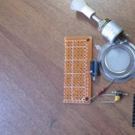
KIT came to build a frequency synthesizer on Si570 with USB control. This synthesizer is planned to be used as part of a future SDR transceiver. The set was ordered. Delivery from the UK to Moscow by regular mail took less than three weeks. On this site you can order a different type of synthesizer with manual frequency adjustment and indication on the LCD matrix. Also, you can buy separately the Si570 chip and much more...
20-04.2014
The synthesizer is assembled and tested - it works. It took about two and a half hours to assemble. Transformer 4:1 did not order additionally. With it, you can get a signal generator with an output of 50Ω and a level of + 10-12dBm and use it as an independent device ...
If you want to make, say, an all-band SDR receiver with an independent synthesizer, a digital frequency indicator and smooth adjustment (up to 1Hz), then this kit will do.

View from the soldering side:

12.06.2014
After buying a soldering station with a hot air gun, the board was soldered again. For soldering planar and SMD components, a hot air gun is an indispensable thing!
16.06.2014
It took a lot of time to sort through the PowerSDR versions to work correctly with this synthesizer in conjunction with a transceiver from UT3MK. Perhaps, I soldered both devices faster than I understood the nuances of the software. In the end (thanks for the tip RA3AIW) the synthesizer started working in the 1.19.3.15 series. Default skin for this version of the program. The driver for the synthesizer under WinXP and the library, which must be put in the program folder. The synthesizer is controlled via USB, a high level is applied to turn on the transmission mode in the transceiver. Synthesizer control program.
26.09.2014
I don’t know what it is connected with (with the layout of the printed circuit board or with the location of the module in the transceiver case), but at some frequencies the synthesizer gives a large number of spurs. When changing the frequency, they do not interfere, but sticks climb out along the panorama on both sides of the tuning frequency. Perhaps when using a 4:1 transformer at the output, this problem will not be to such an extent ...
05.03.2015
The assumption about the synthesizer as a source of spurs turned out to be wrong (the problem turned out to be in the receiving part of the transceiver). The signal comes out quite adequate. Additionally, I installed a 4:1 RF transformer with trifilar winding on the BN-61-2402, according to the attached diagram, getting a 50 ohm output. In general, there are no questions for the synthesizer and for working with software, where the frequency is controlled via USB - the thing that is most suitable and not expensive.
Unfortunately, the existing drivers for WIN7 do not work correctly enough (during frequency tuning, windows with errors constantly pop up). Under XP, the synthesizer works great! I also use the output from it to switch the transceiver to transmit mode.
17.04.2017
I want to say a little about the minuses of the synthesizer and the problems of the PowerSDR version with which it works. Actually, I see two minuses of the synthesizer:
Lack of switching to control band filters;
Under Win7, when changing the frequency, communication with the synthesizer falls off both in the program for controlling it and in PowerSDR (you have to work under XP).
As for the program, here I found a lot of bugs:
ASIO driver support does not work (at least for me under WinXP);
You can work with MME drivers in the telegraph only with a panorama width of 48kHz (if it is more, the signal for transmission breaks, in SSB mode the program can work with a panorama of 96kHz);
The function of quick recording and broadcasting of recorded data in the transmission mode does not work correctly (the recorded signal in the DSB version at zero IF is visible in the panorama, while the reception frequency remains the same);
For some reason, mirror suppression is not calibrated upon reception;
Linking with other software via virtual audio cables also does not work (in version 1.18, for example, there is no such problem);
The program often crashes when changing settings and saving them in the setup;
Sometimes, for no apparent reason, the image on the panorama starts to be displayed in a mirror image (noted at a sampling rate of 48kHz).
Apparently there are other problems that I haven't found yet...
In a word, I decided to try this synthesizer for future designs in order to have everything I need in terms of switching and not be tied to one software version.
To be continued...
SDR transceiver main board ADTRX_UR4QBP_V2
The idea of developing a universal ADTRX_UR4QBP_V2 board came to me as soon as I decided to try connecting my ACER TravelMate 2410 laptop to the ADTRX_UR4QBP board. Reception worked perfectly on the built-in AC`97 sound card, RX / TX switching worked through a USB-COM adapter, but it was not possible to start transmission ... As you know, in most, and I would say in all laptops, sound cards have a combined linear and microphone inputs in one connector. I decided to add another signal relay to the circuit with two groups of contacts to switch the input of the sound card either to the output of the NE5532P op amp in receive mode or to the microphone in transmit mode. The board works with the KGKSDR program. Schematic diagram of the board Fig.1 has not changed much compared to the ADTRX_UR4QBP board, I just added one relay and a stereo jack.
The connection diagram of the ADTRX_UR4QBP_V2 board Fig. 2 is very simple, but still needs some explanation.
Fig.2 
The connecting cable of the COM port is soldered according to the diagram, on the computer side, on the 7th and 5th pins of the connector, we solder the blocking capacitor. Without it, some copies of the boards refused to transmit. We connect the microphone to the "TO MIC" connector of the board if the sound card has a combined input (there is no pink connector on the sound card). Audio cables connecting the board and the sound card of a computer or laptop must be made of separately shielded cores (each core in its own screen) The 3.5mm stereo jack of the cable to the computer input is unsoldered in parallel, and the line-out cable is unsoldered vice versa.This is due to the peculiarity of the board layout, we solder as I wrote above.There may be problems of mismatch between reception and transmission, if you confuse reception with transmission In the settings of the KGKSDR program, do not turn on the inversion of the IQ signal (the checkbox in Option> Tranceiver> Swap I / Q in & out must be unchecked), if you turn it on, the panorama will turn over and the frequency scale will not correspond to reality. Connector "TO LINE OUT PC ”of the board with an audio cable we connect to the line output of the sound card, to the “TO PHONE” connector we connect stereo phones or active computer speakers or some kind of ULF. It is convenient to use an "audio twin" having one "daddy" 3.5mm and two "mothers" 3.5mm. Stereo phones are connected to one of the "mothers", and active speakers are connected to the other, network with the power button. We connect the pedal to the “TX ON” and “GND” connectors according to the diagram, supply power to “+12V” and ”GND”. We connect the “+TX” and ”+RX” connectors according to the diagram. We connect an antenna or a DFT to the input of the "RF IN / OUT" board. A local oscillator signal with an amplitude of 200 ... 300 mV is fed to the "LO IN" connector, the average frequency for the board's operation is calculated by the formula Flo in \u003d Favg. x 4 , where Flo in is the frequency at the "LO IN" input, Fmed. is the middle frequency of the range (the same is set in the KGKSDR program).
Scheme of the board and connections in SPlane 6 format, printed circuit board in Sprint Layout 5 format - DOWNLOAD

AD9851 DDS Synthesizer for SDR Transceiver
In search of a stable local oscillator circuit for an SDR transceiver, based on the ADTRX_UR4QBP and ADTRX_UR4QBP_V2 designs, there were attempts on my part to make a PLL synthesizer on the DDS AD9832. But due to the large number of chip packages and some complexity in setting up, it was decided to make a synthesizer based on the DDS AD9851. The synthesizer can work with any SDR devices that have a built-in LO signal conditioner and a LO frequency equal to F LO * 4. The synthesizer is designed to operate from 300 kHz to 18 MHz, can operate on 6 amateur HF bands (1.9, 3.5, 7, 10, 14, 18 MHz) and has a continuous overlap in the above frequency ranges. Synthesizer control from a computer parallel port (LPT) using the DDS_AD9851_UR4QBP program. The synthesizer has DFT control for 6 bands and quasi-sensor control from the UHF program and attenuator. It makes no sense to describe the principle of the synthesizer, since the most important element in the synthesizer that performs the main function is the DDS synthesizer from Analog Devices AD9851.

The electrical circuit diagram of the synthesizer is shown in Fig. 1
Fig.1

Cable for connecting the synthesizer 10-wire in the screen. Soldered according to the scheme. The cable is reversible, the connectors are of the DRB-25 type (male).
Schematic diagram of cable LPT-SINTEZ

Wiring diagram of the DPF board relay Fig.2
Fig.2

Photo board assembly - 
Band pass filters for main board ADTRX_UR4QBP
When designing the circuit board for band pass filters, attention was paid primarily to the compatibility of this circuit with the main board of the SDR transceiver ADTRX_UR4QBP_V2 and the main board of the SDR transceiver ADTRX_UR4QBP, as well as with the AD9851 DDS synthesizer for the SDR transceiver. The band-pass filters are based on the circuit from the RFE board of the SDR-UA transceiver, which, in turn, is one to one with integrated sub-octave band-pass filters from the RED book "High-frequency Circuitry Handbook". Bandpass filters operate in the frequency range 1.6...21.5 MHz, input/output impedance 50 Ohm. The board has a switchable attenuator "ATT" -20dB and "UHF" +12dB. Schematic diagram of the band pass filters for the main board ADTRX_UR4QBP is shown in the figure.

The scheme for constructing such filters assumes a "beautiful" frequency response with very little attenuation in the passband at the level of -3dB (0.1 ... 1.0dB) and decent attenuation (up to 50dB) outside the passband of these filters. For example, we observe the frequency response of a bandpass filter for the frequency range of 7.3 ... 12.0 MHz, made according to this scheme in the figure below.

The attenuator is made according to the "P-shaped" scheme on resistors R1 ... R3, which is switched on using the relay contacts K13.1 and K14.1 and has an attenuation of -20dB. Relays K13, K14, in turn, are turned on / off by the "ATT" button of the synthesizer control program on the AD9851. The control signal (+5V) from the synthesizer board goes to the Jmp1 connector, the "ATT" contact of the board, and through the DD1 ULN2803 microcircuit, which has 8 keys with protective diodes, controls the attenuator relay. The broadband high-frequency amplifier is made according to the "standard" scheme with correction and using a high-frequency transistor KT368 connected according to the scheme with a common emitter with a broadband high-frequency transformer in the load. Cascade gain (+12dB) is selected using resistor R7, frequency response correction in the region of 13 ... 20 MHz is performed by selecting resistor R8 and capacitor C70. The quiescent current of the amplifier is set within 40 ... 50 mA by resistor R4. Transformer T1 is made on a ferrite ring 600-1000NN Ø7 ... 10mm with a 0.2mm wire into two wires of 7 turns, we connect the beginning of one winding to the end of the other, thus forming the middle output. UHF is turned on using relays K15 and K16, similar to an attenuator. The bandpass filters are similar to the RFE board circuit of the SDR-QU all-band SDR transceiver, they are made on T50-2 and T50-6 ferrite rings of the American company AMIDON. They are switched using relays K1 ... K12, depending on the range. It is possible to use ferrite rings of the 50VCh brand of domestic production Ø12 ... 18mm, if filters are made on such rings with the corresponding values of the inductances of the loop coils given in the diagram, the frequency response of filters made on such rings can be downloaded and viewed in the "pdf" format. The filters are tuned with an NWT-7 frequency response meter from Victor US5CAA. I give winding data for band-pass filters using rings of the American company AMIDON.

And one more thing ... trimmer capacitors for filters 1.6 ... 2.5 MHz, 2.5 ... 4.0 MHz can not be installed, with the "correct" inductance of the coils and the matching of the capacitor ratings in the filters, the frequency response turns out to be "ideal "!!! All relays are domestic RES-49 with a response voltage of 12 ... 13.8 V. The printed circuit board of the band-pass filters is made on double-sided fiberglass of the FR-4 brand with a blue protective mask and marking of the element ratings. PCB drawing in Sprint Layout 5 download.

In the actual design of the transceiver, the size and mounting holes of the bandpass filter board match those of the ADTRX_UR4QBP_V2 board. The filter board is installed on mounting racks above the ADTRX_UR4QBP_V2 board.
All the best and good luck!!!
Power amplifier for SDR transceiver ADTRX_UR4QBP
To build a power amplifier, I spent about 2-3 hours of time, while there is not much time to write ... Therefore, for now, I present the circuit of the PA itself, which I use in my ADTRX design.

Transformer T1 is made on a ring 7 ... 10 mm with a permeability of 1000 NN, 9 turns into two wires without twisting with a diameter of 0.2 ... 0.3 mm.
T2 - type binoculars of two columns of 3 rings with a diameter of 10 mm and a permeability of 1000 NN. Primary winding 3 turns of mounting wire in insulation (wire diameter without insulation is approximately 1 mm). Secondary winding - one turn of PEV or PEL wire with a diameter of 0.8 ... 1 mm.
T3 - type binoculars of two columns of 5 rings with a diameter of 10 mm and a permeability of 1000 NN. The primary winding is one turn of PEV or PEL wire with a diameter of 0.8 ... 1 mm, the secondary winding is 3 turns of the installation wire in insulation (wire diameter without insulation is approximately 1 mm).
The program for the transceiver.
Related Articles